Planar Optical Waveguide PLC Chip
Optical Simulation
Including chip optical index design, waveguide structure refractive index adaptation, BPM optimization
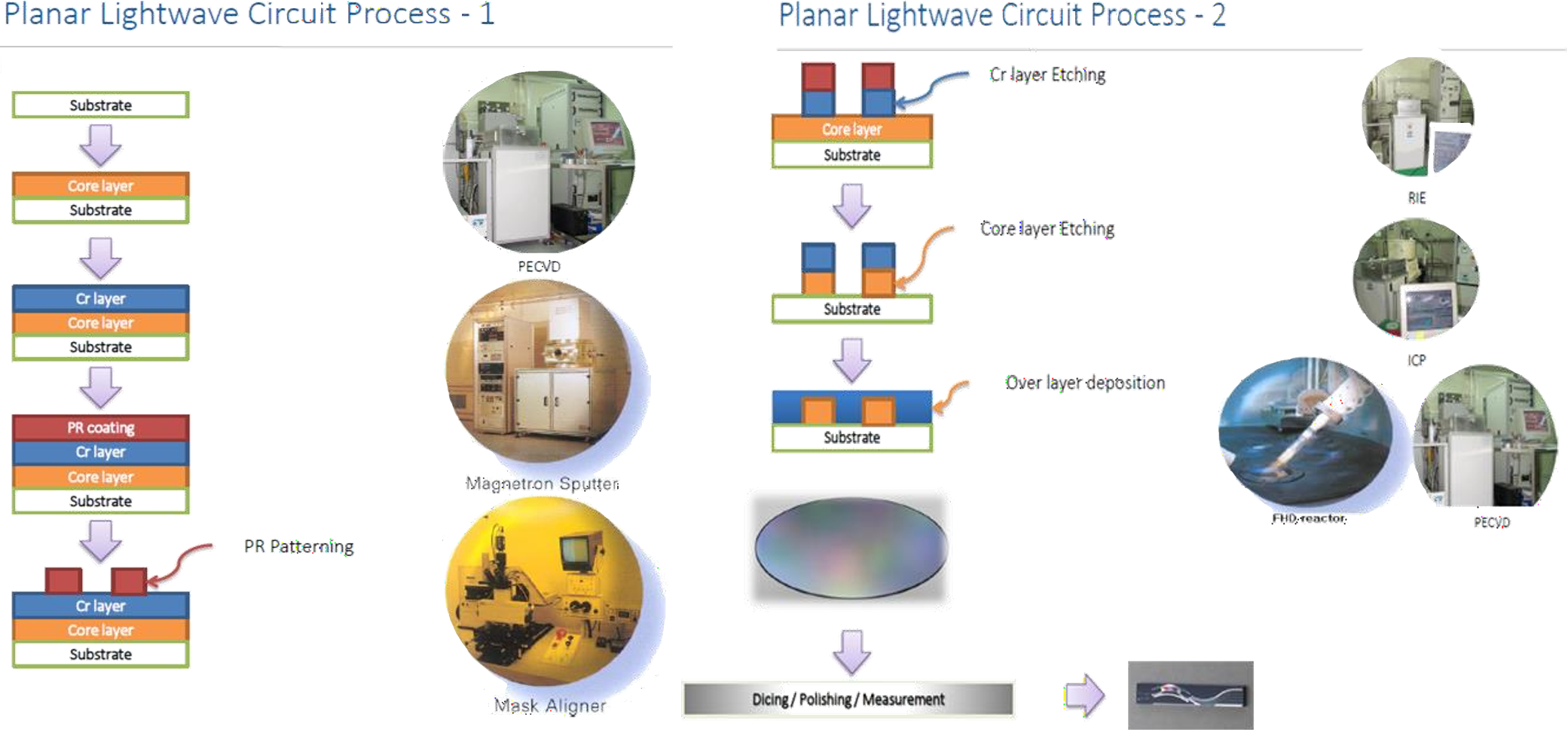
Structure&Process
Advanced semiconductor process technology including PECVD, lithography and etching
Testing and Reliability
Including chip performance test and reliability test analysis capabilities